In a bold move with someone unexpected timing, Intel has officially declared its cutting-edge 18A process node is ready for customer projects. This surprise announcement marks a major milestone in Intel’s aggressive roadmap, positioning the company at the forefront of advanced chip manufacturing. With tape-outs slated for the first half of 2025, Intel 18A is set to revolutionize the industry, challenging dominant players like TSMC and Samsung while opening new doors for AI, HPC, and next-gen computing solutions.
Intel 18A: A New Era of Chip Design
At the heart of Intel 18A are two transformative innovations:
- RibbonFET (Gate-All-Around Transistor Architecture): Intel’s first implementation of gate-all-around transistors, RibbonFET replaces traditional FinFET designs to reduce power leakage and enable higher performance at lower voltages. This approach ensures enhanced transistor scalability and improved energy efficiency — critical for power-hungry AI and HPC workloads.
- PowerVia (Backside Power Delivery): A revolutionary shift in power architecture, PowerVia decouples power delivery from signal routing by shifting it to the backside of the wafer. This not only reduces signal interference but also boosts transistor density and overall performance. Intel is the first major foundry to implement backside power delivery at scale, giving it a competitive edge over industry peers.
Together, these innovations deliver a 15% improvement in performance per watt and a 30% increase in chip density compared to Intel’s previous Intel 3 node.
Why This Announcement Reshapes the Industry
Intel’s readiness with 18A carries massive implications for the semiconductor landscape. The company has been striving to overcome past manufacturing hurdles, and this announcement signals a triumphant step forward.
Competitive Positioning:
For years, TSMC and Samsung have dominated the foundry space, leading the way in sub-5nm process nodes. With 18A (which translates to 1.8 nanometers), Intel is back in direct competition, offering a process node that rivals TSMC’s N2 (2nm) node set for mass production in 2025.

Customer-Centric Foundry Model:
Intel’s IDM 2.0 strategy—a hybrid model combining in-house production with foundry services—is paying off. The 18A Process Design Kit (PDK 1.0) is now complete, enabling external partners to begin designing on the platform. Industry reports suggest that Amazon Web Services (AWS) and Microsoft are already exploring partnerships to leverage 18A’s capabilities for cloud and AI infrastructure.
What Sets Intel 18A Apart?
- AI-Optimized Architecture: With AI at the forefront of technological innovation, Intel 18A is designed to handle AI accelerators, high-performance GPUs, and edge devices with increased power efficiency.
- High-Performance Computing (HPC) Focus: The process node supports massive parallel computing demands, making it ideal for data centers, scientific simulations, and advanced analytics.
- Versatility Across Markets: From mobile chipsets and aerospace-grade components to advanced server processors, 18A offers broad applicability across multiple industries.
Challenges Ahead
While Intel’s 18A announcement is a major achievement, it comes with its share of challenges. Competing with TSMC and Samsung in the foundry business means matching not only their process capabilities but also their economies of scale and production efficiency.
Additionally, as chiplet-based architectures gain popularity (e.g., AMD’s 3D V-Cache and Apple’s M-series SoCs), Intel will need to ensure its advanced packaging technologies keep pace. The company’s Foveros and EMIB packaging solutions are poised to complement 18A’s strengths, but execution will be key.
What’s Next for Intel?
With 18A now ready, Intel’s next focus is on 20A and future sub-nanometer nodes. The company’s roadmap includes:
- 20A (2nm) Node: Featuring the first implementation of RibbonFET and PowerVia (expected to debut in 2024).
- Future Nodes: Exploration of high-NA EUV lithography for sub-1.5nm designs.
Intel is also heavily investing in its foundry infrastructure, with new fabrication plants under construction in Arizona, Ohio, and Germany, aiming to meet growing demand and strengthen supply chain resilience.
Conclusion: Intel’s Path to Foundry Dominance?
The announcement that Intel 18A is now ready for customer projects is more than a technical achievement—it’s a bold statement of intent. By introducing groundbreaking technologies like RibbonFET and PowerVia, Intel is setting new standards in performance and efficiency. If its execution matches its ambition, Intel could successfully position itself as a formidable competitor in the global foundry race.
As the semiconductor industry braces for the next wave of AI, HPC, and quantum computing demands, Intel’s 18A process may very well be the catalyst that reshapes the landscape.
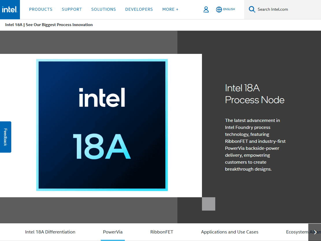
For more information or to explore Intel’s 18A process further, visit Intel’s official page.
Key Takeaways
- Intel’s 18A manufacturing process is ready for customer projects with production starting in 2025
- PowerVia technology introduces revolutionary back-side power delivery for enhanced chip performance
- The complete PDK release enables immediate customer design development for 18A chips
Intel 18A Process Innovation
Intel’s 18A manufacturing process represents a significant leap in semiconductor technology with breakthrough innovations in transistor architecture and power delivery systems.
Technical Advancements
The 18A process node, equivalent to a 1.8nm-class technology, introduces two key innovations: RibbonFET transistors and PowerVia backside power delivery. RibbonFET replaces the FinFET architecture with a gate-all-around design for superior electrical control and reduced power leakage.
PowerVia technology moves power delivery to the back of the chip, enabling improved power distribution and signal integrity. This design reduces power loss and enables higher transistor density.
The Process Design Kit (PDK) for 18A is now available to customers, supporting early design work and optimization through EDA tools.

Performance Implications
The 18A node delivers substantial improvements in chip density and performance per watt compared to Intel 3. Early testing shows promising yields and performance metrics.
Power efficiency gains come from reduced leakage and improved power delivery through the PowerVia system. These advancements enable higher clock speeds while maintaining thermal targets.
Advanced packaging options integrate with 18A, including through-silicon vias for 3D designs. This flexibility allows customers to optimize their designs for specific performance requirements.
Initial customer tape-outs have begun, indicating strong manufacturing readiness and validation of the process technology.
Industry and Market Impact
Intel’s 18A readiness signals a transformative shift in semiconductor manufacturing, strengthening the company’s position against competitors and expanding strategic partnerships.
Foundry Services Expansion
Intel Foundry Services gains significant momentum with the 18A process technology. The advanced manufacturing capabilities position Intel to compete directly with TSMC and Samsung in the contract chip manufacturing space.
The 18A process incorporates RibbonFET gate-all-around transistors and PowerVia backside power delivery, enabling superior performance and power efficiency for high-volume production.
Intel’s foundry capacity expansion includes facilities in Arizona, New Mexico, and Ohio, creating a robust manufacturing network for external customers.
Strategic Partnerships and Collaborations
AWS emerges as a major customer for Intel Foundry Services, providing crucial validation for Intel’s contract manufacturing capabilities. This partnership demonstrates Intel’s ability to serve leading tech companies.
The Intel Foundry Accelerator Ecosystem integrates key players like Cadence and Synopsys, offering comprehensive EDA tools and design services.
US Mag Alliances strengthens Intel’s domestic semiconductor manufacturing presence, aligning with national initiatives to secure chip supply chains.
IDM 2.0 Strategy
Intel’s IDM 2.0 strategy combines internal manufacturing excellence with expanded foundry services. The 18A process supports upcoming product lines including Arrow Lake, Lunar Lake, and Panther Lake processors.
The strategy enables Intel to manufacture chips for logic, mobile, and server applications while maintaining cutting-edge process technology development.
Process design kit (PDK) 1.0 for 18A is ready for customer projects, marking a critical milestone in Intel’s foundry business development.
Frequently Asked Questions
Intel’s 18A node marks significant progress in semiconductor manufacturing with improved performance, power efficiency, and strategic importance for Intel’s foundry business.
How does Intel 18A performance compare to TSMC’s equivalent node?
Intel 18A aims to compete directly with TSMC’s 2nm process technology. Early test results indicate promising performance metrics, though specific benchmarks remain private.
The node demonstrates Intel’s renewed focus on manufacturing leadership. Intel claims performance advantages in key areas like power consumption and transistor density.
What are the expected benefits of Intel’s 18A process to the semiconductor industry?
The 18A process provides access to advanced manufacturing capabilities through Intel Foundry Services. This creates more options for chip designers and manufacturers.
Companies can now use Intel’s cutting-edge technology to produce their own semiconductor designs. The increased manufacturing capacity helps reduce supply chain bottlenecks.
When is the Intel 18A node scheduled for mass production?
Intel has confirmed successful early chip boot-ups on the 18A process. The first products using 18A technology are now sampling to customers.
Mass production is expected to begin in 2025. The company has released the complete Process Design Kit 1.0 to foundry customers.
What advancements does Intel 18A offer over previous semiconductor technologies?
The 18A process uses advanced transistor architectures and manufacturing techniques. These improvements enable higher performance and better power efficiency.
The node features enhanced gate-all-around transistors. Manufacturing refinements allow for increased transistor density compared to previous generations.
Are there any reported production or yield challenges with Intel 18A?
Initial testing shows positive results with the first two products successfully booting. Intel has not disclosed specific yield numbers from early production runs.
The company reports steady progress in development phases. Early customer feedback appears encouraging based on test chip performance.
How will Intel’s 18A process impact future computing and electronics?
The advanced manufacturing capabilities enable new chip designs for AI, mobile devices, and high-performance computing. More powerful and efficient processors will drive innovations across multiple technology sectors.
The process supports development of specialized chips for emerging applications. The technology advances computational capabilities while reducing power consumption.